(Yet another!) Nintendo Space Fever PCB repair
I think I must have 'Space Fever' Fever! Why else would I try to bring yet another Space Fever PCB set back from oblivion? It's not even really a set, just some loose PCBs in non working, not even complete condition.
There's a CPU PCB which seems complete except for the actual CPU and EPROMs, a Colour and a Black and White I/O PCB both missing various components. Either of those I/O boards could be used with the CPU PCB to suit their respective monitor type, assuming they are repairable...
That only leaves the sound PCB to make up a set so I've been very kindly offered the spare sound board from my previous, Space Fever Colour PCB repair. I will also need a pair of the 50 way IDC interconnect cables, I can make up some new ones or borrow a pair of similar cables from one of the other PCB sets in my growing 'to be repaired' pile.
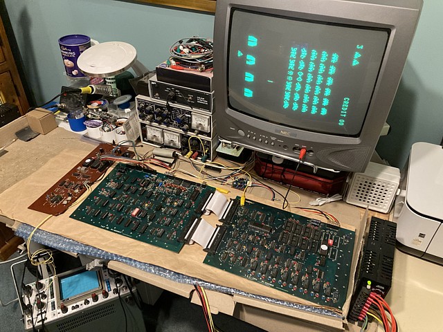
I still have the working Space Fever Colour PCB set which I repaired earlier set up on the bench so it will be much easier to test and repair this CPU PCB in conjunction with the working I/O and sound boards then use it to repair the other two I/O PCBs. That's the plan, at least.
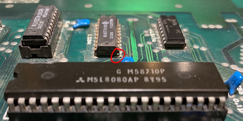
So, to begin I'm installing a pre tested 8080A CPU IC and the full set of original Space Fever 2708 EPROMs from the previous CPU board, these are not verified and may contain errors but will provide some activity at least. I have repaired the two broken pins which the G1 EPROM suffered on removal from its socket by soldering new legs (cut from a faulty IC) onto the remaining stubs on the EPROM.
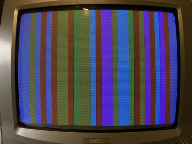
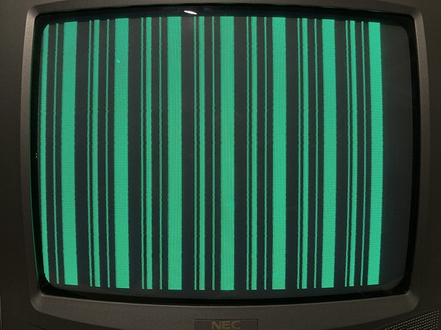
Connecting the CPU board to the working I/O and sound boards and power supply rails via my bench test lead, powering on there are just some coloured bars on screen but I wasn't expecting much as yet. There are sure to be some problems which sidelined the board in the first place and after years of storage many more potential issues.
Checking the Voltages and signals around the 8080A CPU all the Voltage rails and the two clock signals are present, there is some activity on the address outputs but none on the data lines, they all appear to be sitting at an intermediate Voltage and not a valid High or Low TTL logic level. It could be the CPU is attempting to read data from the program EPROMs but the data returning via the buffer ICs is invalid or possibly floating.
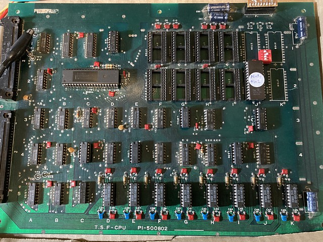
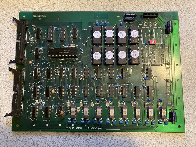
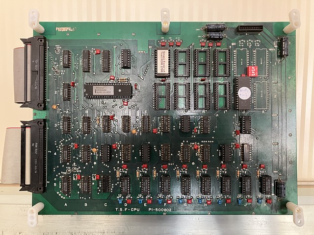
This CPU board is a model 500802 and uses a pair of 74LS241 buffers but is otherwise similar to the 500810 CPU PCB which I repaired previously. That model used a pair of 8216 buffers, some of the component locations may also vary between the two versions but they are functionally the same.
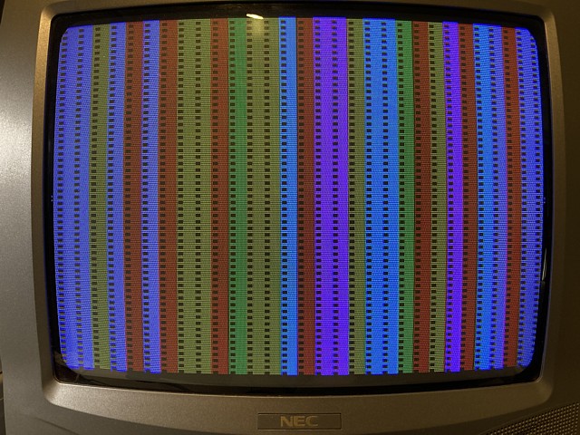
Now checking the control signal to the buffer ICs which selects the direction of data flow - this comes from the CPUs DBIN control output via a 74LS04 inverter in position 4E, it seems the inverter is at fault with a valid signal at its input pin 1 but none at its output pin 2. Replacing the inverter, adding a socket there is now some activity on the data lines and a slight change to the image on screen but the program still freezes at an early stage.
So the CPU now appears to be receiving program data from EPROM but are the EPROM ICs being correctly addressed by the CPU? Comparing the Address signals from the CPU to the inputs of the address buffers (actually 74LS08 AND gates, being used as buffers in this instance) there's a problem. Some of the address signals from the CPU are not present at the inputs of the buffers.
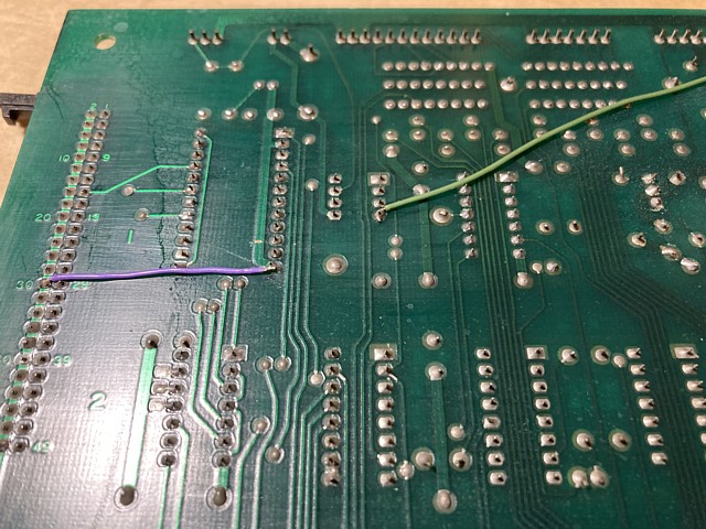
Following the tracks and testing for continuity it turns out the CPUs 40 pin IC socket has some bad contacts and needs to be replaced.
I'm attempting to repair some non working and incomplete Nintendo Space Fever PCBs in the hope of assembling a complete working board set, beginning with the CPU PCB. So far I've replaced a faulty 74LS04 inverter and found some poor contacts on the original 40 pin CPU socket which I've now also replaced. Powering on once again there is a very slight change to the image on screen.
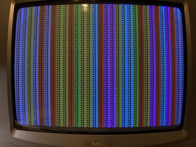
That may not seem like much of an improvement but each fault found and corrected is one step closer to a working PCB. Admittedly we may have a few steps yet to travel. The slight change to the image on screen suggests there was some additional CPU activity but the pattern remains static so the program must have stalled at an early stage.
Checking the CPU address lines once again, this time they appear to be completely idle. Testing CPU control signals, the READY input signal is stuck low which has left the CPU in a wait state. The READY signal comes from a 74LS74 flip flop in position 3E, testing its inputs it seems its /CLEAR input, pin 13 is being held in the active low state.
This in turn comes from a 74LS00 NAND gate in position 3G but that IC also seems to be responding correctly as both of its inputs are high. One of those inputs is derived from Address line A14 which we know is idle, the other comes from a 74LS08 AND gate in position 4C. Checking the inputs to the AND gate, one is low while the other is pulsing so we would expect the output to be low but it measures high.
So it seems the 74LS08 is faulty but removing it, adding a socket and replacing the IC does not change the result at its output. It would appear that signal is either shorted to +5V somehow or the input of a following IC is faulty, pulling the signal high. Testing with a multimeter I can see no continuity to the +5V rail so I'll try replacing the 74LS00 in position 3G which has the signal at its input pin 1.
Still no joy unfortunately so checking the circuit diagram once again the signal in question which is labelled ST STB on the diagram also connects to the clock input of the 74LS174 latch IC in position 1D. There doesn't seem to be any other connection which could be holding this signal in the high state so replacing the 74LS174 seems to cure that problem. The READY signal is no longer being held low and the CPU now appears to have some activity.
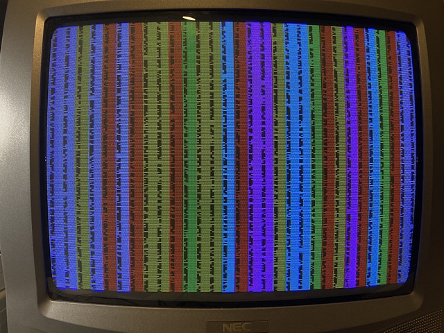
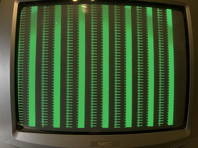
This time those black columns on screen are not stationary, the pattern changes but does remain within the columns. Looking closely at that information it appears the black patterns are two pixels wide with distinct, seemingly random information at the left and right side. If we ignore the colour overlay which is generated on the working I/O PCB we are seeing a 'white' screen with two adjacent bits from each byte containing random looking (black) information.
Initially I guessed there were two bad RAM ICs responsible for this pattern but I got that wrong. Now checking the signals around the RAM all have the three Voltage rails and ground, address activity, row and column address strobe signals and the read /write signal is toggling. These inputs are the same for each RAM, being bussed across all 8 IC positions.
Looking at their individual data inputs and outputs now, each of the RAM ICs has active data at its input but only two, in positions 5E and 5F have valid data on their output. The outputs of the remaining RAM ICs are either stuck high or at some intermediate level and not a valid logic state. It seems 6 of the 8 RAM chips are bad, the two with active data at their outputs appear to be the good ones.
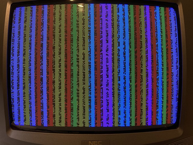
To try and confirm this I'll remove the first IC from position 5D whose output was stuck high, install a socket and plug in a known working component. Having done that and powering on again the result is similar but we can see the column of black patterns is now 3 bits wide, the remaining 5 bits still blank or 'white' prior to the colour overlay and seen as various colours on screen.
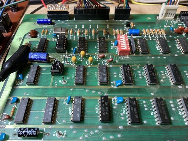
Normally if I found a bad RAM IC or two I would just remove and replace the faulty components, adding a socket to those positions in the process. In this case however the majority of the RAM seems faulty so the extra effort to carefully remove all of the 4116 ICs and socket the entire RAM area seems worthwhile. With a slight modification to the PCB tracks I can fit a full set of new old stock 4164 ICs in place of the original 4116 type.
The 4164 RAM should be more reliable, only requiring a single 5V supply as well as easier to source replacements if needed. Although each IC has 64k x 1 bit capacity as opposed to 16k for the 4116, in this configuration the extra memory space will not be accessible by the CPU, the additional row and column address line being tied high and not active. Having all of the RAM area socketed should also simplify any future troubleshooting with the ability to easily substitute a known good component for any of the on board RAM ICs.
So after removing all of the 4116 ICs. socketing and substituting a set of the 4164 RAM, powering on to test there's still a memory problem. Only the first five consecutive bits appear to have activity on screen, the last three still blank. This time however the outputs of the 4164 ICs all show some activity when tested, the 74LS08 buffer in position 4I now seems to be the point where the activity is lost. Replacing that IC restores the flow of data and for the first time we have a meaningful display on screen.
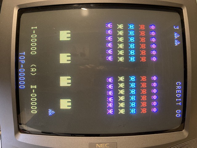
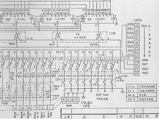
The image looks good and attract mode is running but there are no missiles on screen and the game does not add credit when the coin input is operated. Checking the circuit diagram, the coin input signal is read from the I/O PCB along with the player 1 inputs, controlled by the /IN0 signal. Similarly, the missile positions would be read from the shifter circuit on the I/O PCB by the /IN3 signal.
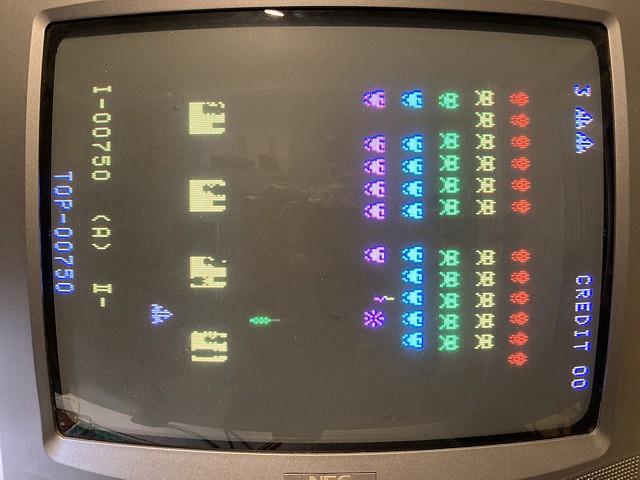
The input strobes /IN0 to /IN3 originate on the CPU PCB from the 74LS139 in position 3J. Checking that IC the signals at its inputs all appear active but none of the outputs have valid signals. Replacing the IC cures that problem. The game now coins up and plays correctly, player controls working and missiles appearing correctly on screen.
My Nintendo Space Fever CPU PCB is working now but still running an original set of 2708 EPROMs which I've borrowed from another Space Fever board set. Now those PCBs are also repaired the plan is to convert the original EPROMs to the High Splitter version and refit them in their original locations so I'll need a replacement ROM set for this PCB.
I don't have any spare 2708 EPROMs and my programmer doesn't support that type, I'm working on an adapter to reprogram those existing EPROMs for their original PCB but for my own board I can combine the individual ROM files and program those on to a larger, single EPROM. One 2764 8k x 8bit EPROM can accommodate the entire Space Fever ROMset, in this case I'll be using a single 27256 EPROM with a DIP switch to select one of four 'ROM banks' within its total 32k x 8bit capacity.
That will allow the PCB to contain multiple versions of software which were designed to run on this hardware including the original Space Fever, its High Splitter variant and Space Launcher. I'm also intending to write some diagnostic / test software for this CPU and hardware configuration, that's a future project but will fit into one bank of this EPROM compilation once complete.
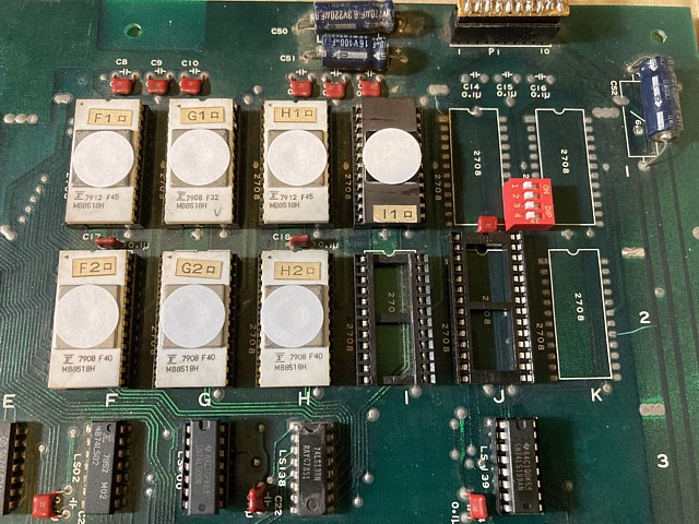
The single EPROM and DIP switch can be fitted to some unused positions within the original CPU PCB layout, these appear to have been configured for additional ROM in the 8k - 12k address region but not required for Space Fever or its variants. The 27256 EPROM is a 28pin device instead of 24 pins for the 2708 but there is sufficient space to fit a 28 pin socket with minimal modification allowing any additional wiring to be added to the solder side of the PCB.
The DIP switch fit neatly into some unused PCB through holes which have been repurposed with 4 x 10k Ohm pullup resistors to one side, switching to ground on the other. Switch 3 and 4 are used for 'bank select' while switch 2 enables the single EPROM, also disabling the original EPROM positions or vice versa. This allows a full set of original EPROMs to be fitted and still work on the PCB or alternately the single EPROM can be used, as selected by DIP switch No. 2.
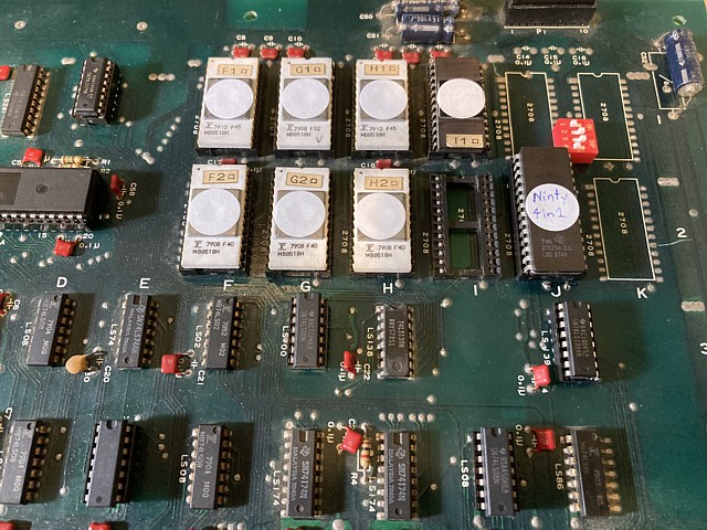
The CPU PCB with modification complete, seen here with the single EPROM selected and running Space Launcher. In order to hear the correct sounds for each game there is a corresponding (but much simpler) modification required for the sound PCB which is yet to be done, using a 2732 4k x 8bit EPROM to replace the original 2708 sound EPROM.
Having tested the operation of the repaired Nintendo Space Fever CPU PCB and single EPROM modification along with its ability to select either the original ROMset or the single EPROM, the original 2708 EPROMs can now be removed to be reprogrammed and returned to their original PCB. With the CPU PCB now working we can move on to the first of two I/O PCBs to be repaired.
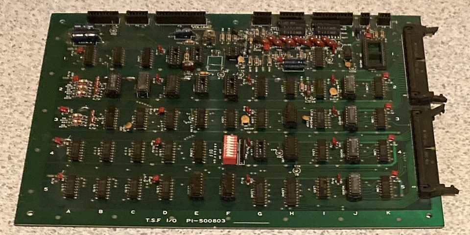
We'll begin with the Colour I/O PCB, type 500813. Although the PCB itself appears to be in reasonable condition there are several components missing, it would seem the board had been reduced to a parts donor but should still be repairable as it stands. Apart from the missing components there are some which have been damaged or broken due to poor storage or handling so we will sort out all of those issues prior to testing.
The first item conspicuous by its absence is the original 20.160 MHz crystal. I've searched for this frequency before with no luck for another Space Fever PCB repair, eventually settling on a standard 20 MHz value which is within 0.8% of the original frequency and close enough to work without any noticeable difference. So I already have a few of those on hand for this exact purpose.
Other missing components around the clock generation area are the 74LS164 and 75361A ICs from positions 1B and 2B. I had already ordered some replacements on initial inspection of these PCBs which have since arrived so installing those with new sockets along with a few 4.7uF Tantalum capacitors which were also missing, that section now appears complete.
Checking the rest of the PCB there's a 10uF Tantalum capacitor missing from the corner nearest the control inputs. Fitting a new one and moving on to components which have been damaged a 2SC828 transistor was bent over with one leg broken, replacing that and there are four axial electrolytic capacitors on board which were badly scuffed during storage - when boards are stacked without any packing between them the sharp pins on the bottom of one PCB will damage or scratch components on the board underneath.
None of those capacitors was squashed or so badly damaged they would likely not work but to tidy up the PCB it seems worthwhile replacing them. Axial electrolytic caps are less common than the radial type so needed to be ordered in. I've replaced a 33uF and a 47uF so far, will replace the 100uF and 220uF ones when they arrive from order. Meanwhile the existing ones should work OK, I've tested the PCB for shorts between any of the Voltage rails and ground just to ensure there are none.
One more issue I noticed, a number of the small signal diodes in the area of the sound control outputs had cracked or chipped glass bead packages. When tested with a multimeter they all appeared to be working but just to be sure I decided to replace them. The original type was 1S2075K and checking its ratings the common 1N4148 seems a good substitute which I have on hand. For consistency I'm replacing all the diodes of that original type on board, D1 to D7.
So, with the I/O PCB now looking complete with no obvious defects it's time for testing. The initial result is promising, there is sync at least but no image just a black screen. Checking the Luminance signal at TP9 there is activity there so the issue is likely to be in the final stage where the colour overlay is applied to the luminance (black and white) signal to create the R, G and B outputs.
The luminance signal is fed to three inputs of the 74LS00 NAND gate in position 4F, each gate driving a single output colour and the other input of each gate being controlled by the colour overlay circuit. When checked though the luminance signal was not reaching any of the 74LS00 input pins due to a socket / contact issue. It seems this component had been previously replaced and a poor quality socket added.
In addition to the poor socket contacts the ICs pins were a bit rusty so the best solution was to remove and fit a new socket and new 74LS00 IC. Having done that the video output appears, attract mode running and colours looking correct. Finally testing the game control inputs and sound control outputs to the sound PCB the game is running, playing and sounds correct.
I've been attempting to revive some Nintendo Space Fever PCBs which I bought in a non working, incomplete state. The CPU board and the Colour I/O PCB are now fully working which leaves an earlier version Black and White I/O PCB. Lets see if we can get that one working as well.
There doesn't seem to be any readily available documentation for the black and white version but I've read that the Colour I/O PCB is very similar apart from the addition of the colour overlay circuit. So the colour I/O schematic will be very useful for troubleshooting but some of the ICs PCB locations will differ between the two versions. I'll make a note of any differences encountered as I go along.
The PCB doesn't look too bad but has obviously had a lot of repair work done with several of the ICs having been socketed at some point. Seven of the sockets are empty, the ICs having presumably been used as spares for other PCB repairs. Thankfully the sockets themselves appear to be of reasonable quality with double wipe contacts and are not looking tarnished or corroded so hopefully it will just be a matter of installing replacement ICs into the existing sockets.
Fortunately the type numbers of the missing ICs are noted in the PCB screening next to each empty socket so it was straightforward to order replacements which have now arrived. Before I install the replacement ICs though, I'll remove each of the remaining socketed ICs in turn and test them using the logic IC test function of my EPROM programmer.
This section of the PCB has a number of issues to check and resolve. Firstly, the IC in position 2B was a 74HC174 rather than the expected 74LS series component. The 74HC series are TTL compatible CMOS components and should work in place of the original part but I prefer to fit the original spec. component where possible so will replace this IC with a new 74LS174. Out of interest I did test the IC which I removed from the PCB and it was reported as working.
The next IC in position 2C is also supposed to be a 74LS174 although the type number printed on the PCB is difficult to read and the markings on the IC itself almost obliterated by scuffing. It turns out the correct component was fitted but the real issue in this instance is the incorrect fitment with two of the IC legs missing the socket completely.
Given the poor appearance of the component I would probably have replaced it had I not just used my last spare 74LS174 in the adjacent position so instead I removed it from its socket, straightened the legs and tested the IC was working before reinstalling it correctly.
Another remnant from a previous repair are the solder bridges which span a number of cuts across the PCB tracks carrying the +5V supply to the ICs in rows 2,3,4 and 5. This was a short cut (no pun intended) method of locating a component which would have been shorting the supply rail. The power rail to each row would be cut in turn, once the row was identified which carried the short circuit (row 2 in this case) further cuts along the row would pinpoint the short circuit.
Once the short circuit was removed the cut tracks would be re joined with solder and possibly some wire spanning the cut, to restore the supply to all of the components. In this instance the joins across the cut tracks are not too messy so I'll just test the +5V supply rail for continuity and to ensure no shorts remain, if that all seems correct I'll leave them as found.
Continuing with repairs to the Nintendo Space Fever Black and White I/O PCB I've tested several of the existing socketed ICs using my EPROM programmer's logic IC test function, fitted replacements for the missing ICs as well as a new 20 MHz crystal to replace the original 20.160 MHz one which was missing and also replaced a few of the axial electrolytic capacitors for good measure.
There are still a few messy solder joints here and there from previous repairs but it's time to connect the PCB to my working CPU board, power it on and see what we get.
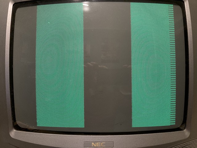
The green screen is expected as the Black and White version of Space Fever only had monochrome video with separate, positive going sync so won't work with the composite video input on my NEC TV. I'm using a test lead which I made for a previous repair which connects the sync via a transistor inverter and the video signal to the green input only on my TVs RGB input.
The pattern on screen however leaves a lot to be desired. There's not a lot going on there, it appears the CPU may not even be running so the next step is to check the clock signals etc. which are generated on the I/O PCB and necessary for the CPU to run.
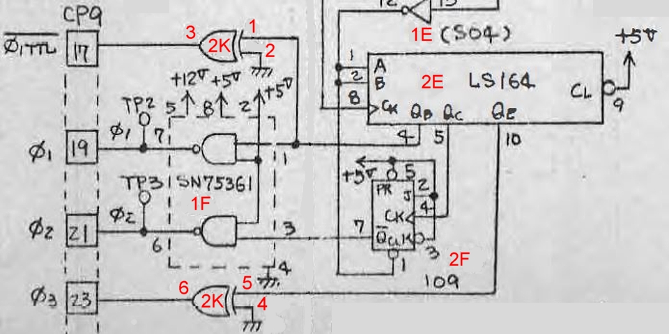
There are test points on the I/O PCB for the two 12V clock signals to the CPU, these appear to be present and correct and there should also be two TTL level clock signals which control other devices on the CPU PCB. Using the Colour I/O schematic as a guide and tracing the actual connections on the Black and White PCB, the component locations and pin connections for the black and white version are marked in red on the drawing.
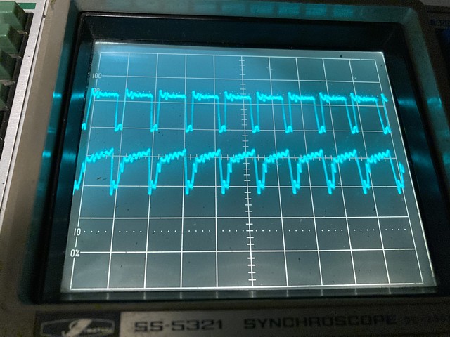
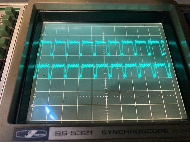
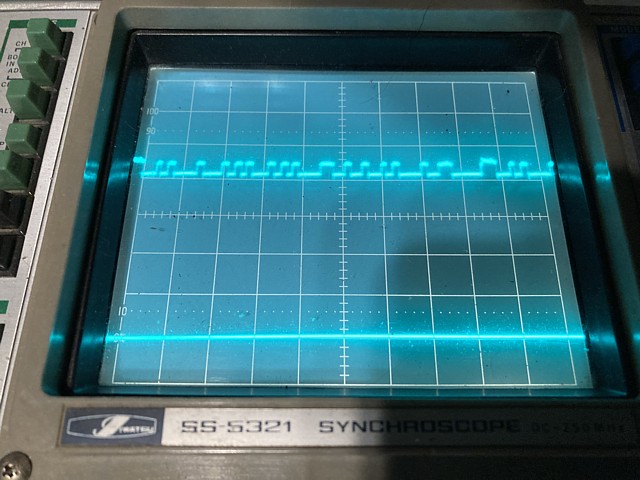
The TTL level clock signals are buffered by a 74LS86 in position 2K, both appear correct at its input pins 1 and 5 but the phase 3 signal from its output pin 6 looks incorrect with a very long rise time (lower trace, the input signal at pin 5 is seen in the upper trace).
That definitely looks like an IC on the way out so removing it, installing a socket and a new 74LS86 the clock signals now look correct.
Incidentally, the signals look a bit noisy on the display but that's not really an issue, I've just connected my oscilloscope ground to the ground test point on the PCB with a wire rather than using the short ground wires on the oscilloscope probes. The setup does pick up a bit more noise but is quicker and safer than having to find a ground point for the probes very close to the point being measured.
Having corrected that clock signal however does not make any change to the main issue. Moving on to the Power On Reset circuit (labelled PCL on this board) the signal to the CPU should go High briefly upon power up then return to a logic Low state while its inverted /PCL signal should go Low briefly then return to a High state. The circuit on the Black and White PCB is similar to the Colour version, once again tracing the actual connections the part locations and pin numbers are shown in red.
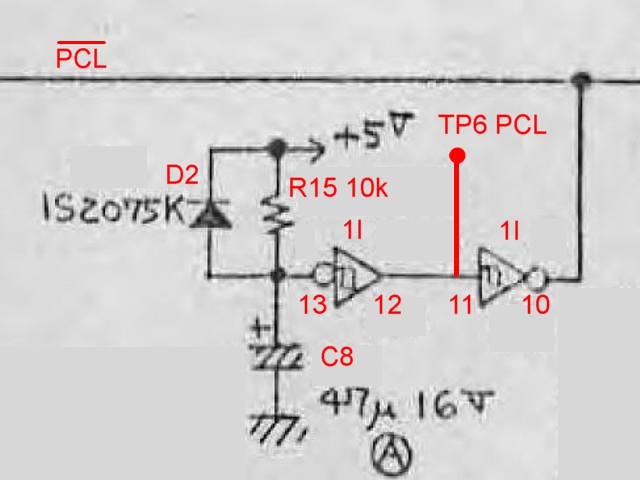
Looking at the PCL signal at the output of the 74LS14 Schmitt trigger inverter in position 1I pin 12 I can't see the output going High at power on, even if its input pin 13 is held low with a link to ground the output remains low. So, replacing the 74LS14 and adding a socket corrects the reset issue. We now have some CPU activity.
I'm making progress with the third of three Nintendo Space Fever PCBs which I'm attempting to resurrect, the CPU and Colour I/O PCBs already working and this earlier Black and White I/O PCB now showing signs of life...
The program seems to be running correctly but there are some graphics issues, the missiles just showing as a couple of blocks and there are some glitches which appear on the screen soon after power on. The game does coin up and play but the two player flip screen function does not seem to be working. That could be a fault or perhaps the PCB was modified at some stage, early cocktail games were sometimes modified by operators to work in upright cabinets where flip screen operation was not required.
I'm not sure if the graphics glitches and the incorrect missile images are related but we can start with the missiles as it is often easier to trace a fault which is consistent than one which seems to appear at random. Although much of the graphics content is generated on the CPU PCB (which is known to be working), some of the motion is handed over to hardware on the I/O PCB where a bank of TTL ICs perform some of the graphics shifting operations to save on CPU calculations which could slow the program flow.
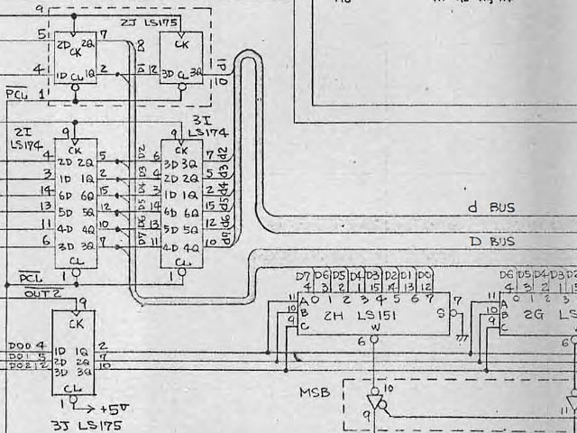
The section of the I/O PCB which performs this task includes a bank of 8 x 74LS151 8 input multiplexers, on the Black and White version these are found in locations 4A, 4B, 4C, 4D, 5A, 5B, 5C and 5D. Looking at the signals on their inputs there seems to be no activity at all. Tracing back, the data and control signals arrive from the CPU PCB via a set of latches and the clock signals for the latches all appear to be stuck in a logic Low state.
Tracing the stuck signals further back these come from a 74LS42 decoder, on the Black and White I/O PCB this is found in position 1C. Sure enough its outputs are all permanently Low - they should default to the High state, only one selected output being Low at any given time. Replacing the 74LS42 gets those output strobe signals working which improves the appearance of the missiles on screen but only slightly.
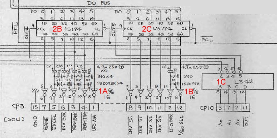
The 2 player flip screen operation does now appear to work correctly, it turns out this was controlled by the 74LS174 flip flop in position 2C, pin 15 which is now active due to the restoration of its /OUT5 Strobe signal. The other outputs from the pair of 74LS174 ICs in positions 2B and 2C control the sound PCB, at this stage I'm running the CPU and I/O PCBs without the sound PCB connected and will move on to troubleshooting any sound problems once the graphics issues are sorted.
Getting back to the input data at the multiplexer ICs most are now active but one of the data bits, at input pin 4 of the 74LS151 in position 4A is stuck at about 1 Volt and not a valid logic level. This traces back to the 74LS175 flip flop in position 3B, pin 2 so replacing that IC, also adding a socket corrects the missing input data.
Looking at the output data on pin 6 of each multiplexer now only four of the eight ICs have a valid output signal the remainder having outputs stuck at an intermediate, invalid logic level. These are buffered by a pair of 74LS368 ICs in positions 4E and 5E and the marginal levels at their inputs could possibly be causing the glitches on screen as well as the still incorrect appearance of the missiles. I don't have any 74LS151 ICs on hand or 74LS368s for that matter so will need to order some as well as more sockets.
It's becoming clear that there was widespread damage to the components on this PCB, possibly caused by a monitor arcing or a power supply going too high. Perhaps this explains why a previous attempted repair may have been abandoned, at the time the board may have been more easily replaced or used as spares to fix another board with a less extensive fault. Either way we've made too much progress to give up now, a few more parts and a little more work should have it running again after many years in limbo.
Continuing with repairs to the Nintendo Space Fever Black and White I/O PCB, the 74LS151 ICs have now arrived from order. Replacing the four which had low level outputs appears to have restored the operation of the shifter circuit, the missiles and moving objects now looking correct. That has not resolved the other issue where glitches appear on screen so the next step is to try and trace their origin.
A few pixels flickering on screen may seem like a pretty minor issue but these can be the most difficult faults of all to trace. Rather than a signal which is incorrect or missing entirely, a graphics glitch is often caused by a signal which is noisy, has marginal levels or timing which is not quite perfect.
To begin with I'll ensure the power supplies are well filtered by replacing the remaining two electrolytic capacitors on board, for the +5V and +12V rails. The original axial capacitors in these positions were 220uF/6.3V for the +5V and 100uF/16V for the +12V. I ordered replacements which were listed as being available from stock but to date those have not arrived so I'm substituting the nearest (larger) value which I have on hand. These ones are 470uf/25V and should work equally well in this instance.
In this part of the PCB there was a deep scratch across one of the major ground tracks, left by a previous 'repairer' who had been cutting the nearby +5V rail at various points and apparently had a slip of the blade. I wasn't sure if the copper had been cut all the way through so cleared away some of the solder mask on either side of the gouge and flowed some solder over the full width of the track to ensure good conductivity.
That done and re-testing, the graphics glitch remained as before so moving on to search for other possible causes, there is a clue to the section of the PCB where the problem may be originating.
Looking at the image as the attract mode runs, at the very beginning the image is clean with no errors. This seems to confirm the video output from the CPU PCB via the 74198 shift register on the I/O PCB is working properly. As more text is added the glitches appear. This occurs each time the attract mode loops around to the same point.
This coincides with a burst of activity on the 'DI' data bus between the I/O and CPU PCBs. The bus contains multiplexed data being read by the CPU from the I/O board which includes control inputs, DIP switch settings and graphics data returning from the shifter circuit. If that graphics data is corrupted or the switching between sources is not timed correctly the errors would carry through to the video output which could explain our glitches on screen.
The graphics data is selected onto the bus by a pair of 74LS368 ICs in positions 4E and 5E while the control inputs and DIP switch settings are via 74LS240 buffers in positions 5G and 5H. Their selection is by signals /IN0 to /IN3 which originate on the CPU PCB. As the CPU board worked correctly with the colour I/O PCBs repaired already it should be safe to assume the select signals themselves are not the cause of the problem.
Looking at the multiplexed data on the 'DI' bus, the signals do appear to have a lot of high frequency noise which could be causing errors - a TTL signal must be 0.8V or less to be a valid logic low so an IC output of say 0.5V would be correct but add about 0.5V of noise and the signal may not always be detected as 'low'.
It's difficult to tell the exact source of the noise as the outputs of the individual buffers are all connected together to the data bus. To see if the 74LS240 buffers are working at all I can change their inputs by setting the DIP switches and selecting control inputs with a wire link to ground while observing their outputs with an oscilloscope.
That seems to confirm the buffers are functioning but then I notice that the glitches on screen disappear when any of the player 1 control inputs are selected with a wire link to ground. Looking with the oscilloscope the noise level does seem to decrease when any of the inputs are grounded so I'm wondering if the 74LS240 in position 5G is the source of the noise seen on the data bus.
As a precaution I'll install sockets and replace both 74LS240 buffers just in case both might be contributing to the noise on the data bus. Disappointingly that appears to make no real difference, at least I have ruled out one more possible cause. Now I notice another clue - when I first tested the inputs with a ground wire that wire was connected to a nearby ground test point TP3 on the CPU PCB. Now double checking the inputs, this time I have just linked them to ground on the same I/O PCB connector, P6.
The result is not the same, when connected to ground from the CPU PCB the glitches disappear completely while connecting to the local ground the glitches improve slightly but still remain. That seems to prove there is a significant difference between the two grounds.
The ground on both PCBs start out the same as both come from the same point on the power supply, via a pair of connecting cables. Each arrives at the opposite side of the PCB and is carried across the board by a number of tracks both on the component side and solder side. Each logic IC connects to the +5V rail and ground, drawing a little current and inducing some high frequency noise onto the supply and ground rails. There are also regularly spaced 0.1uF ceramic / monolithic capacitors connected between +5V and ground to absorb some of this noise.
There are about 5 capacitors for each row of ICs or about 1 for every second IC, one possible way to reduce the noise levels would be to double the number, placing a capacitor across the supply to each IC. Another way of course would have been to reduce the resistance of supply and ground tracks by increasing their width wherever space permitted.
The problem seems to be that the ground level on each PCB at the point nearest the interconnecting cables has accumulated a significant amount of noise. The noise on either side is not identical so there is a slight potential difference (i.e. a small AC Voltage) between the ground on the two PCBs. When a logic signal passes from one PCB to the other via the interconnect cables the difference in the grounds is effectively added to the signal, resulting in some errors or glitches.
The ground from the CPU PCB is carried over the interconnect cables, in fact almost every second wire is grounded presumably to reduce crosstalk between signals on adjacent wires. But the grounds are not connected at the I/O PCB side. I'm guessing this was designed to prevent ground loops which are a common issue in lower frequency circuits where the current drawn through the ground return path of a signal can induce a small Voltage which adds noise to the output, for example hum in an analog audio environment.
But the issue here is high frequency noise and a more effective solution seems to be a brute force approach, ensuring the ground has the minimum resistance. It could be that the solder joints along the PCB have deteriorated over time and are not as effective as they once were - there are many vias or plated through holes in the PCB connecting the ground tracks from one side of the PCB to the other which may not be as conductive now as when new. In any case the best solution seems to be to connect the two grounds and eliminate the potential difference between them.
A short wire link added from the CPU ground on the interconnect cable to the nearby I/O ground. Having done that and viewing the signals on the 'DI' bus as well as the ground the amount of high frequency noise appears to be significantly reduced. As expected the glitches on screen are gone.
Incidentally the green wire in the photo carries the ground for the 24V coin counter directly from the power input to the switching IC, presumably to prevent a spike on the logic ground when the coin counter is triggered. It appears to be factory installed as there is no PCB trace connecting that pin to ground originally.
So I'm calling this PCB repaired even though it took a little modification to make it work properly, causing me to wonder how it ever worked originally. As a footnote there are some other factors which may be relevant; firstly the original machine used a linear power supply whereas I'm using a switchmode supply which could increase the high frequency noise on board.
Also the PCBs are originally mounted either side of a metal plate which is grounded to the machine cabinet and could help to shield high frequency noise as opposed to spread out on the bench with very long wires for power connection.
I have used the same test setup to repair other Space Fever PCBs, both Colour and Black and White without similar issues however looking back on previous photos I now realise the Black and White I/O PCB previously repaired was a different model number.
This PCB is a model 500803 while the previously repaired model was 500811 so now I'm wondering what the exact differences were between them. Neither has any documentation available as far as I know and I don't have the other PCB here to compare. The layout appeared to be pretty similar but I assume there must have been some change to justify a new part number, perhaps some revision for known issues with the earlier PCB.
For the moment that remains a mystery. Meanwhile I've just picked up a second CPU PCB also in non working condition so while I still have the test setup on the bench let's see if we can get that one happening as well.
I'm working on some Nintendo Space Fever PCBs which I've recently bought in a non working, incomplete state having also been stored for many years. Their prior history is unclear but they seem to have come as part of a job lot from an arcade operator in the day with a number of previous repairs or repair attempts already evident. I'm guessing at some point the repairs were abandoned and the boards subsequently used as parts donors for other games still in service.
So far, I've repaired one CPU PCB as well as a Colour and a Black and White I/O PCB. Having managed to repair both I/O PCBs it seems worthwhile to try and tackle a second CPU PCB repair. Of course I initially picked the best looking repair prospects so each additional repair attempted is likely to be more difficult than the previous!
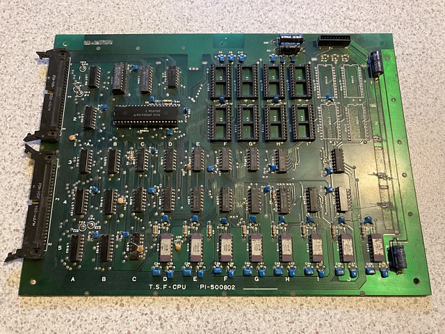
This CPU PCB is another type 500802, with the 74LS241 buffers in position 1B and 1C. Judging by the residue on the PCB both of those have previously been replaced though only one was socketed, more on that later. There are also obvious scars from the +5V rail which leads to the rows of components having been cut at various points and then roughly rejoined as part of a previous repair attempt, most likely to locate a component which was shorting the supply rail.
For the moment I'll just test to ensure no shorts remain but leave the rejoined tracks until I've had a chance to properly test the operation of the PCB. If they are not causing a problem at present I'll leave those as found until any other faults are sorted and just tidy them up later. Meanwhile the 8080A CPU and all of the EPROMs were missing, for the CPU I'm fitting a spare (which as yet is untested) and for the EPROMs I will make a slight modification to the PCB and substitute a set of 2716 2k x 8 bit EPROMS for the original 2708 type.
An important difference between the 2708 and the newer 2716 or 2732 EPROMs is the 2708 uses +12V and -5V power supplies on pins 19 and 21 in addition to the +5V Vcc supply on pin 24. To substitute a later part these two supplies must be disconnected from the EPROM sockets. On this PCB there is a pair of tracks on the component side inbetween each EPROM position which can be neatly cut (near the top of photo above).
Both the 2716 and 2732 type EPROMs use pin 19 for the additional address input A10 and the 2732 has one more address line A11 on pin 21. To use just a 1k Byte section of their capacity as a substitute for the 2708 these additional address lines can be tied to a logic low or high or they can be switched to allow more than one software set to be contained within the EPROMs and selected using a DIP switch.
I've added a 2 way DIP switch to an otherwise unused position on the PCB as seen in the photo above. And below, the two additional address lines are connected to +5V by 10k Ohm pullup resistors but can be held low by the DIP switch which connects them to ground. Using a set of 2732 EPROMs this would allow selection of four 1k Byte ROM 'banks' within each 4k x 8bit EPROM.
In this instance I'm using 2716 EPROMs so only require a single switch for address input A10. Pin 21 on this device is for the Vpp programming Voltage and should just be maintained at +5Volt during normal read operation. Using the 10k Ohm pullup resistor turned out to be insufficient to hold this input on all eight 2716 EPROMs to a logic high state so for the 2716 I've removed the wire from the second switch and instead connected it directly from pin 21 on the EPROM sockets to the +5V Vcc rail.
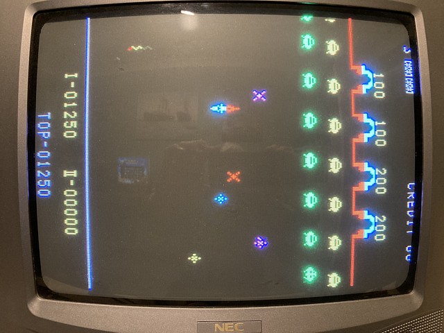
I've programmed a set of eight 2716 EPROMs with the original Space Fever ROMset also placing the High Splitter version into the upper 1k Byte of each. The original Space Fever only occupies seven EPROMs while the High Splitter version requires eight so the lower half of the eighth EPROM contains no data. Having done that, powering on and double checking the power supply Voltages to ensure all are still at nominal levels here is the initial output on screen.
That's pretty much as expected so heading straight to the CPU and checking power supply Voltages, clock signals, reset signal and then looking for address and data activity the first untoward result is from data bit D3 which seems to have no activity. That's not necessarily a CPU problem, assuming the processor is still attempting to read its instructions from ROM it could be no data is being received via the 74LS241 buffer in position 1C.
Checking the buffer pins 11 and 12 which are supposed to connect to D3 on the CPU there is activity there so we're looking at a connection issue and the assumption is (another!) bad CPU socket. Replacing 40 pin IC sockets is a pretty tedious job so just double checking for continuity using a multimeter it turns out the CPU socket is OK (glad I checked!). Instead the problem is a lifted track under the buffer IC which was damaged when the IC was previously replaced and is not connecting to pins 11 or 12 as it should.
Once a track has been overheated and lifted from the PCB the copper is quite thin and has no strength so the most reliable repair is by adding a fine wire to make the connection directly. Ideally the components at either end of the wire should be socketed so any future need to replace either component does not require the wire repair to be disturbed. So instead of just adding a wire I'll remove the IC, add a socket, probably replace the IC while I'm at it and add the fine wire to ensure the connection is reliable.
I don't have any 74LS241 ICs on hand at present and would prefer to wait until I can order in some spares so will just do a temporary repair to join the lifted track to the pins with a blob of solder on the component side of the PCB. It's messy but does restore the connection so I can proceed with troubleshooting the PCB. I'll fix it later, promise!
Powering on again there's just a little more activity before the display freezes. Rechecking the signals around the CPU the data bits now all appear active, moving on to the address outputs all are present but the A0 signal from pin 25 is only about half the amplitude of the other outputs.
On the oscilloscope at 5V per division the A0 signal appears to range between about 1V and 3V, this could be a faulty CPU or an excessive load on that particular output pin. A0 is buffered by the 74LS08 AND gate in position 3D so I'll try replacing that and see if the signal level improves.
No change unfortunately so it seems that 8080CPU does have a fault after all. Rummaging through my component spares I have found one more spare 8080A IC, this one is an Intel original and dates from 1979. Installing that and re testing the address and data lines are now all active with correct Voltage levels, the image on screen remaining active briefly upon startup then once again freezing.
Now that all the signals around the 8080A CPU are present and levels appear correct it's time to extend the search for issues which could prevent the program from running. A quick check of the signals at the input and output of each 4116 16k x 1 bit RAM IC shows all are present, a good sign so hopefully all eight of these original components may still be functioning correctly. There could still be RAM errors but for the moment we'll look for problems elsewhere.
Returning to the CPU data bus, this is bidirectional at the CPU end but the 74LS241 buffers have a separate path for data being sent from the CPU and data received from other sources via a set of 74LS153 multiplexers. So the activity which seemed correct at the CPU may just be outgoing data while some of the incoming data could be incorrect or missing entirely.
There are four multiplexers, each handles two of the eight data bits and switches between four data sources. Checking the outputs from the multiplexers on pins 7 and 9 of each IC, both signals from the 74LS153 in position 3B are incorrect with only about 1 Volt of signal (lower trace, below) comparing to the same pin on the IC in position 3A (upper trace).
That is a definite fault so removing the component, fitting a socket and a new replacement 74LS153 the outputs look correct and the program now runs. There are still some issues to sort though, beginning with the missiles which just appear as moving blocks.
Repairs to the Nintendo Space Fever PCBs are progressing with the second CPU board now running. There are some issues yet to solve, the missile graphics which initially just appeared as moving blocks have since disappeared completely. Those two symptoms could relate to the same fault or two separate problems, it's not uncommon for additional faults to occur when a PCB is first run after a long period of disuse.
Both symptoms are familiar, scrolling back to the first CPU board repair the complete absence of missile graphics was caused by a missing /IN3 signal from the 74LS138 IC in position 3J. In this case the /IN0 to /IN3 signals are present so what else could cause the graphics data from the shifter circuit not to be displayed?
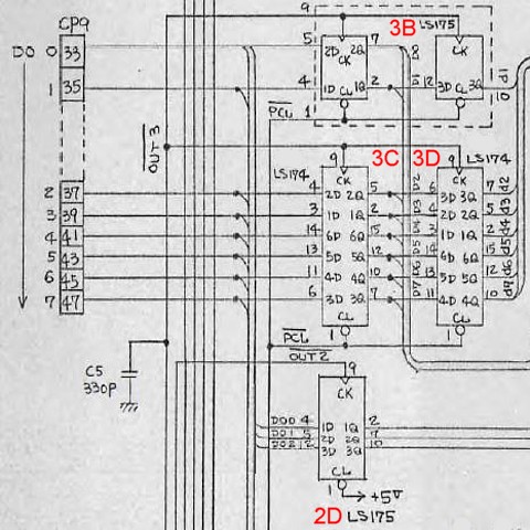
The data from the shifter circuit returns via the 74LS153 multiplexers so checking their control inputs it seems the data from the I/O PCB is not being selected. Tracing the control signals back via the 74LS32 IC in position 5C to the 74LS174 in position 1D that IC appears to have a dead output. The IC in this position had obviously been replaced at some point but not socketed and the component fitted was a 74174 rather than the LS version specified in the circuit diagram.
I've purchased some new 74LS174 ICs as well as the previously mentioned 74LS241 buffers from a local supplier so will replace both components, with new sockets and tidy up that earlier temporary repair in the process.
Having replaced the 74LS174 the missile graphics are now back on screen but they are still displayed as moving blocks so there were evidently two separate faults.
Looking back on the previous repair of the Black and White I/O PCB, a very similar problem was caused by a missing /OUT3 signal which is used to latch data from the CPU PCB into the shifter circuit on the I/O PCB. This time the fault must be on the CPU PCB so tracing all the way back, the /OUT signal which controls data sent to the I/O PCB originates on the CPU PCB from the 74LS00 NAND gate in position 3G.
Checking the output from that IC, pin 8 the signal appears noisy with low Voltage levels so removing it, adding a socket and replacing the 74LS00 cures that issue. The missiles now look correct on screen so moving on to coin up and test the game operation all graphics, controls and sounds appear to be working correctly.
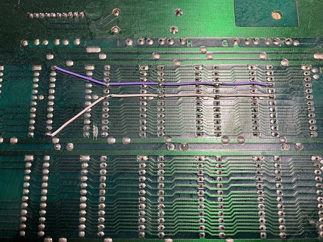
Just to finish this repair off I'll tidy up those previously cut and rejoined tracks which although working were quite messy. I've laid some fine wire braid over the gaps and reflowed solder over the bridge to ensure a reliable connection.
I also noticed some small signal tracks nearby which had suffered a deep scratch, although each still had continuity when tested I've removed some of the solder mask from either side of the scratch and flowed solder over the tracks which will hopefully strengthen them and reduce the chance of failure.
Having done that I'm calling this repair complete. That makes two Space Fever CPU boards, one Colour and one Black and White I/O board all revived and saved from potentially being scrapped.
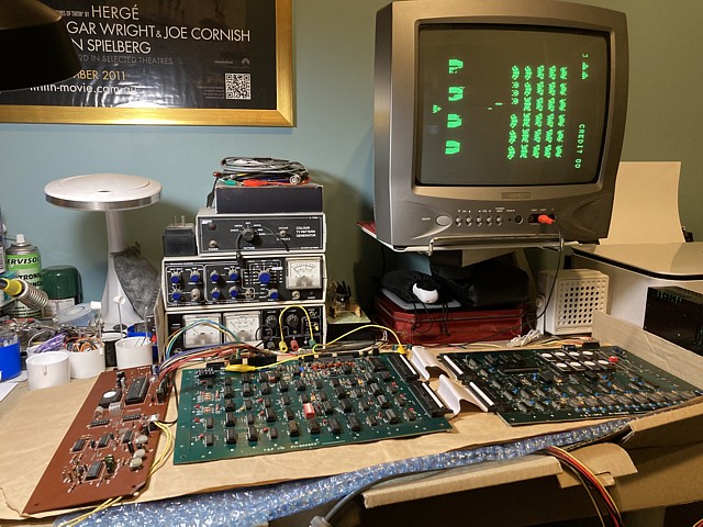
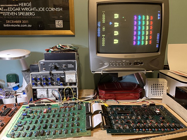
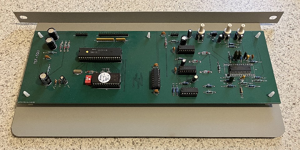
This is just a little update to my previous Space Fever PCB repairs. Recapping on progress to date (scroll back to see the complete story) I bought and repaired two Nintendo Space Fever CPU PCBs and two I/O PCBs, one of those was the colour version while the other was the earlier black and white type. I also repaired one original Space Fever sound PCB and assembled a reproduction sound board using an open source PCB design, with a few revisions. More on that later.
As I left them, both PCB sets were complete and fully working. Just recently I returned them to the test bench to assist with a Nintendo Sheriff repair and noticed both sets have since developed some new, minor fault symptoms. That wasn't an immediate issue as I only needed to take some measurements around the video output section of both types but having done that I will now sort out those new problems while I still have the board sets on the test bench.
The black and white set plays correctly but a couple of sounds are now missing, most notably the UFO hit tune as well as some of the invader marching sounds. That could be a sound PCB problem but could also be caused by a fault on the I/O board. The colour PCB set runs and gameplay is correct with sounds all present but the missile graphics now appear broken, this is typical of an issue with the shifter logic circuit on the I/O PCB in that set.
Let's begin with the colour set. The CPU PCBs are interchangeable between the two sets but as I have them currently configured the colour set has the CPU PCB which I previously modified to use a single 27C256 EPROM and is switchable between 4 game selections. The selections are; the original Space Fever, the High Splitter version, Space Launcher (another Nintendo game based on Space Fever hardware) and the 4th selection was intended for a diagnostic program.
At the time I hadn't yet written my homebrew test ROM software for Space Fever so that program is not currently loaded on to the single EPROM on the CPU PCB. I should really add that by reprogramming the 27C256 EPROM but I do have an original type 2708 EPROM with the test program so I can just place that in the original 'boot' ROM position and use my additional DIP switch to select the original ROM space instead of the single EPROM.
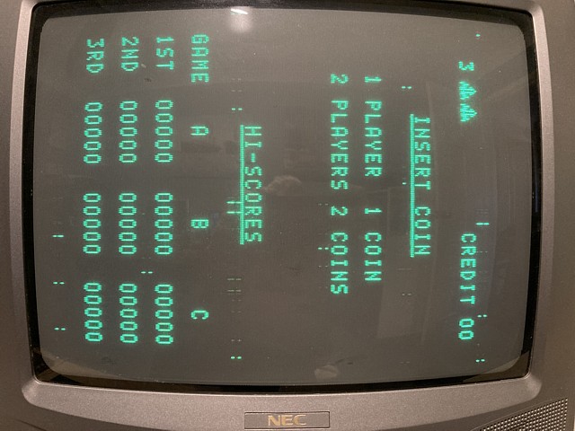
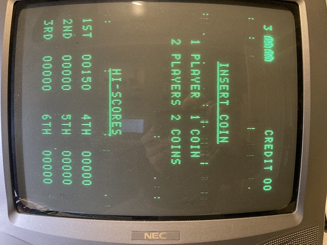
My homebrew test ROM checks the RAM on the CPU board then goes on to test the shifter operation on the I/O PCB. It does that by sending data to the shifter circuit with incrementing shift amounts while comparing the actual result to the predicted value using the CPU to perform the same operation. To date I have tested the test program in MAME as well as on a working Space Fever PCB set but haven't yet tried it with a PCB which has an actual shifter fault so that will be interesting:
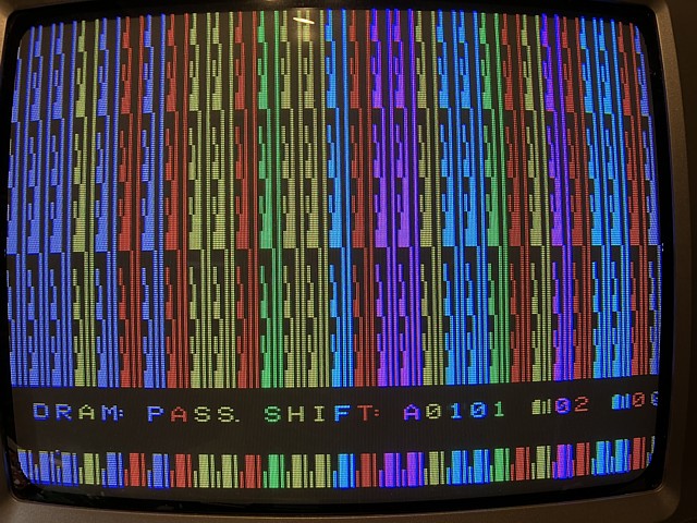
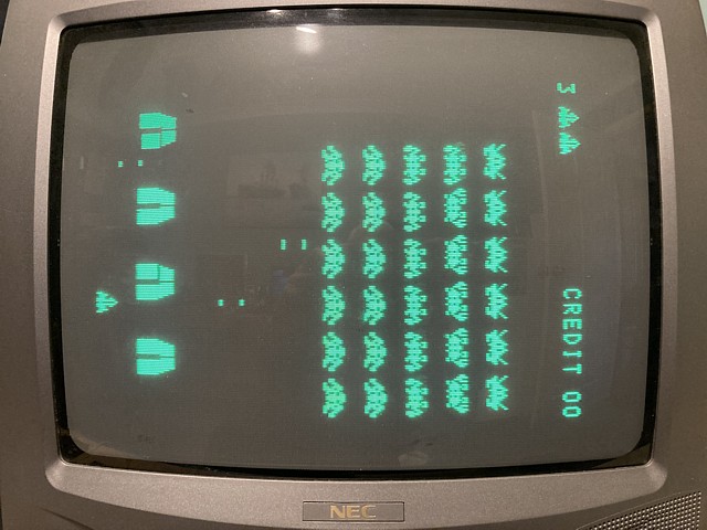
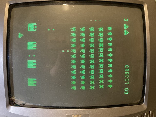
So as expected the CPU RAM passed its tests but the shifter test failed. The results can be read on screen, my test bench monitor is overscanning but the data value read back is just visible as 00. What do those numbers mean? For the shifter test the A value represents the data byte followed by the shift amount from 00 to 07. The next value is the calculated data result using the CPU to perform the shift operation and the final number is the data value read back from the shifter circuit.
In this case taking a data value of 01 and shifting it to the left by 1 bit the expected result would be 02 but we have read 00. That suggests a fault in the area around the 74LS151 in position 3G, which produces the result for data bit 1. Checking the signals around that IC as the test repeats up to the fault position I can see activity on its 3 select inputs as well as its data input for position 1 but its (inverting) output pin 6 has no activity, remaining high.
So I'll try replacing the 74LS151 in position 3G; the good news is that corrects that particular error code. The bad news is the test program moves on and fails the very next input permutation with data 01 and shift amount 02, the result should be 04 but once again 00 is read from the shifter output. Replacing the 74LS151 in position 3G has definitely corrected the initial error so does this mean the corresponding IC in position 3F is also bad?
Once again there is nothing obviously wrong with the inputs to the IC in question yet its output remains inactive so I'll bite the bullet and replace it. And in a repeat performance the error is cured only to move on to a failure in the next shift position. I can't imagine a whole row of ICs have failed as this board set was fully working when last powered up, perhaps there is an issue with input signals which I'm not seeing and the replacement ICs are a bit less fussy about the signal levels or timing.
The data values and shift amount are stored in latches and these signals are connected to the 8 x 74LS151 multiplexer ICs, each responsible for a single output bit. As such the latches are operating with a high fan out where each output is driving a load of 8 inputs. 74LS series ICs can usually cope with a fan out of 10 but one of the latches could have a weak output or one of the multiplexers could be loading the signals abnormally.
Having a closer look at the signals from the latches while the test program repeats up to the point of error, the 3 bit shift value from the 74LS175 in position 3J appears to have normal activity and signal level. The data bits sent to the multiplexers up to this point are mostly zeros as the test does one pass with input value 00 (the result in this case is always 00 as well) then fails when the data value is set to 01. Correspondingly the data bits are all zero (low) except for a brief high signal on data bit D0.
D0 comes from the 74LS175 in position 2J and I can see activity, the level does appear a little low so I'll try replacing that IC. Unfortunately the fault is unchanged and that signal level remains a bit low so the issue is most likely caused by one of the 74LS151 inputs loading the signal down. But which IC? It isn't necessarily the next one in the sequence, in position 3E which now reports an error - any of the remaining original 74LS151s could be responsible for the excessive load on the signal.
Checking all of the 74LS151s to see if any are hot or any signal appears different I finally notice one in position 2E has an output level which seems low compared to the other ICs. This wasn't identified by the test program as the output was still a valid logic level but does suggest the IC is not operating normally and could also be responsible for loading the input signal. Sure enough, replacing that IC corrects the fault and the shifter test now completes without errors.
So although the test program was working and correctly identified the error condition it was unable to pinpoint the exact component responsible in a less common situation where one IC was loading a signal which then caused a different IC to produce an incorrect result. In fact if I had been viewing all of the 74LS151s with equal suspicion instead of focusing on the one which produced the error identified by the test program, I may have noticed the faulty IC with the low output Voltage sooner.
I guess the moral of that story is a diagnostic program can be a useful tool but doesn't always answer that most popular question - 'Which IC do I need to replace to make it work?' Here endeth the lesson...
I've had both of my previously repaired Nintendo Space Fever PCB sets back on the test bench to sort out a couple of new issues which seem to have cropped up since their last use. After some tribulation I have sorted the shifter problem with the colour PCB set so will move on to the missing sounds from the black and white set. This problem should be fairly straightforward compared to the intricacies of the shifter circuit.
Most of the sounds are triggered by an individual output from the I/O PCB, two x 7416 hex open collector inverters are used to drive the outputs with pullup resistor banks connected at the sound PCB end, the sounds being triggered when an input is switched to ground. A few of the sounds are triggered by combinations of outputs so an individual output failure can cause more than one sound to be affected.
In this case the 'UFO Brk' sound is missing as well as some of the faster Invader marching sequences. As the outputs are open collector with pullup resistors it will do no harm to manually trigger the sound with a wire to ground from the UFO Brk output, CP3 pin 2. This does indeed cause the UFO hit sound to be heard so the fault is not on the sound PCB but within the output section of the I/O PCB.
Looking at the circuit diagram some of the output inverters are driven directly by the latches and some including the 'UFO Brk' signal via a capacitor with a resistor to ground to produce a momentary pulse. Using the oscilloscope to view the signal on pin 11 of the 7416 IC in position 1B while playing the game there is a clear pulse on that input when the UFO is hit but no sound or activity on the IC output pin 10. So the 7416 is definitely faulty.
Not having any of these ICs on hand I ordered a few from an overseas seller online but that parcel appears to have disappeared en route. The last tracking showed the package had landed in Sydney but there has been no delivery or update since. I believe the local delivery method is untracked, by post and the package will probably turn up eventually, meanwhile I was making up an order from Mouser for some other parts so added a couple of ICs to that order.
Mouser did have the 7416 IC in stock and also the 7406 which is a pin compatible IC just having a higher output Voltage rating so either will work fine. As it happened the 7406 was less expensive than the 7416 so I went with the higher spec. component for a lower price. The Mouser delivery arrived very quickly, exactly on schedule and replacing the faulty 7416 with the new 7406, also adding a socket has restored the UFO hit sound as well as the missing invader marching sounds so this PCB set is fully working once more.
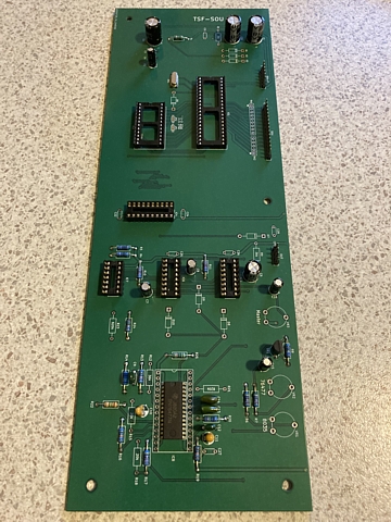
- I mentioned earlier that one of my Space Fever PCB sets has a repaired, original TSF-SOU PCB while the other uses a reproduction sound PCB which I assembled from an open source PCB design. The design was a prototype and untested at that stage but looked fairly complete so I decided to have some PCBs made up, assemble, test and hopefully correct any remaining issues.
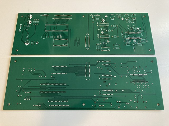
I believe some fully assembled, working and ready to use reproductions are already available from Mikes Arcade and maybe elsewhere but the exchange rate and freight from U.S. to Aus. is usually prohibitive so building up a PCB locally seemed a better alternative from my point of view. Anyway it looked pretty complete so I figured it would probably work with minimal changes, if any.
It turned out there were some unresolved bugs in the design which I was able to correct with some minor modifications so I'll document those here, just in case anyone else has made up some PCBs of the same revision and would like to get them running. This is not a reflection on the designer, who clearly stated that the PCB was untested. I was happy to take the risk and attempt to help by resolving any issues I found and provide feedback, which I did.
The first issue was the 2SC711 pinout. I did source a couple of 2SC711A transistors to use so didn't bother searching for a substitute but it turned out the pinout on the PCB is reversed. Perhaps it was designed with some other substitute transistor in mind. Looking at the flat side of the transistor the pins are B,C,E and the 2SC711 on an original sound PCB is the same so I just put the transistor in backwards and it works fine.
The next was SOU 3 the laser base explosion sound didn't work properly. This was an error in the original circuit diagram showing IC5 pin 3 /CLR connected to pin 15 R/C - but on the original PCB it is just tied high, to pin 16. I had already fitted a socket for IC5 but was able to cut the track from pin 3 to 15 and add a link on the solder side from 3 to 16 which got that sound working.
Then the 8035 didn't seem to work at all. Initially I thought the crystal clock pins were working OK but when I double checked the frequency it was free running at about 1/10th of the correct 6MHz. Turns out there was too much capacitance from those pins to ground. The original PCB uses 2 x 30pF ceramic caps from pins 2 and 3 to ground - and works OK but these are actually higher than Intel's recommended values for crystal oscillator mode.
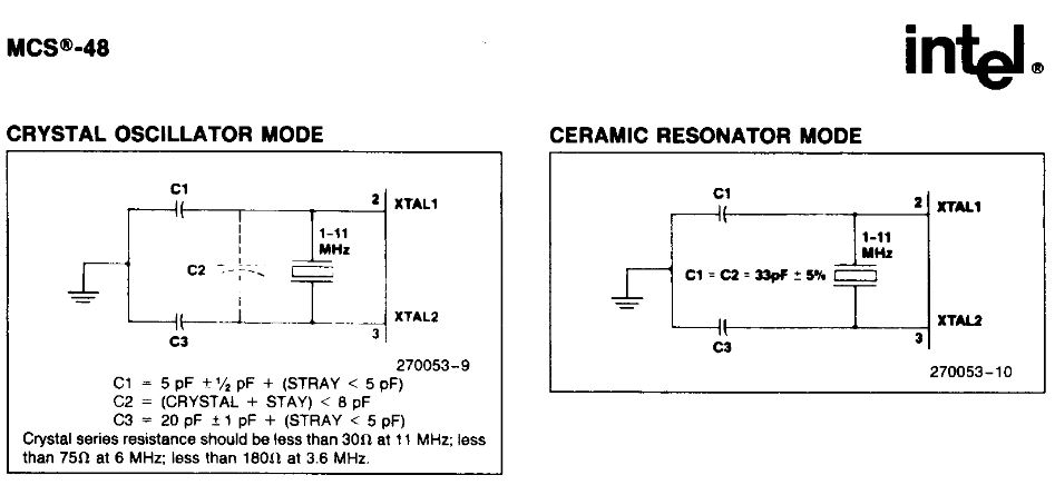
I think this PCB being double sided with ground planes on both sides adds a lot of stray capacitance, I actually removed both C3 and C4 completely which got the clock running at the right frequency but I ended up using 4.7pF for C3 and 18pF for C4 which were the nearest values to the recommended ones, allowing for some stray capacitance and those worked out OK.
That got the clock working but the controller program still wasn't running. Tracing the address latch, all seemed OK bt the data returning from the EPROM to 8035 had bits 0-7 reversed. That's probably because DB0-7 for the 8035 on the Nintendo diagram are shown the wrong way round. Rather than cut the 8 tracks and rewire I just used a hex editor to reverse the data bits on the entire ROM file, which worked equally well for the prototype PCB.
That done, the PCB seemed to be working OK just testing each sound by grounding the input pins. Once I tested it with the Space Fever board set I did notice one more odd behaviour, when shooting at invaders which were very close to the laser base there was no hit sound as the firing sound was still active. Turns out this was another thing on the Nintendo circuit diagram which was not quite as it appeared.
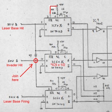
Two wires which look like they just cross on the circuit are actually connected on the original PCB. SOU 6 which goes to IC6 pin 10 on the original PCB (on this PCB it goes to IC5 pin 10) should also connect to IC6 pin 3 and D7 anode. This gives the hit sounds priority over the firing sound so if the invader is very close the hit sound will be heard over the firing sound. Added a wire link and now it does work correctly!
There was one other modification which I added to enable alternate sounds for use with other game ROMsets. The Space Fever PCB set can run other versions such as the Hi-splitter variation and Space Launcher, each of these use alternate sound EPROMs so it's possible to use a 2716 or 2732 with a pullup resistor on the additional address pins and switch to ground to select the appropriate sound set.
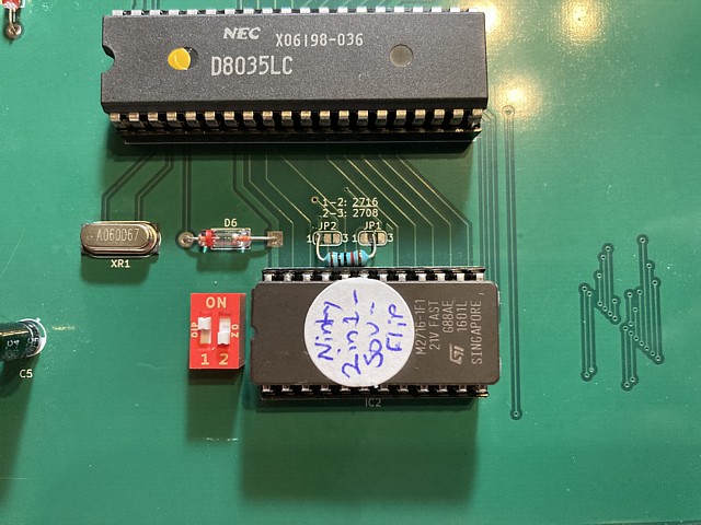
I've used a 2716 with the Fever and Hi splitter sounds so added a link from A10 to a DIP switch, the second pole of the switch could be wired to A11 if a 2732 was used. One pin from each pole of the DIP switch is connected to the ground plane, the other is insulated with some small tubing and a slightly larger through hole drilled to prevent contact with the PCB ground.
Another issue with the original TSF-SOU PCB as well as this reproduction is the original Nintendo design took a few short cuts to reduce the IC count, using some diodes to combine signals along with an open collector inverter. That worked OK, mainly because they chose 1N34 germanium diodes to keep the Voltage drop across the diode junctions to a minimum. That was fine in 1979 when you could still obtain germanium diodes but genuine ones are hard to source now...
I know Shottky type silicon diodes have a fairly low forward Voltage but they also have a significant reverse leakage current which may be an issue with this design. I didn't really try any alternatives, just sourcing some n.o.s. germanium diodes in this case. If I was designing a new PCB from scratch a 3 input AND gate might be a better solution than the marginal diode design of the original. Just a thought!
Anyway, I only needed one sound PCB to complete this board set so the prototype one with those small changes should be fine - I'm very happy to have a (new) fully working sound board to complete my second Space Fever set.
That completes the Space Fever PCB repairs, for now at least and frees the test bench for some new PCB repairs, to follow soon...
Web Resources (External Links) -
Nintendo Space Fever Colour repaired PCBs test running Hi Splitter ROMset - YouTube
Space Fever (colour version) interconnection pinouts - CrazyKong.com
Reproduction of the TSF-SOU sound pcb - Github.com
All images and text on this website are Copyright.
Contact: jbtech at telstra dot com